OVC's JFS Laboratory achieves silicon photonics integration breakthrough
JFS Laboratory, based in the Wuhan East Lake High-tech Development Zone (Optics Valley of China or OVC), has illuminated a laser light source integrated into a silicon-based chip, marking the first successful implementation of this technology in China.
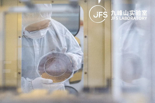
Utilizing its proprietary heterogeneous integration technology, the JFS Laboratory completed a complex fabrication process for integrating an indium phosphide laser within an eight-inch SOI wafer.

JFS Laboratory achieves its breakthrough in silicon photonics integration. [Photo/WeChat account of Optics Valley of China]
This technology uses optical signals with superior transmission performance and is crucial to revolutionizing inter-chip signal data transmission.
Its primary objective is to address the current physical limitations of inter-chip electrical signal transmission. This innovation is set to revolutionize data centers, computing power centers, CPU/GPU chips, AI chips, and related fields.
As the standard climbs for information transmission and processing, traditional microelectronics technologies struggle to tackle issues like power consumption, heat dissipation, and crosstalk within chips. In contrast, optical-electrical heterogeneous integration technology enables high integration, low cost, and high-speed transmission.
This technology effectively addresses the current technical bottlenecks in microelectronic chips and is a crucial way for the information industry to surpass Moore's Law-based technologies.


