Weifang 3D Printing Technology Innovation Center
About the investment promotion unit
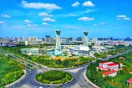
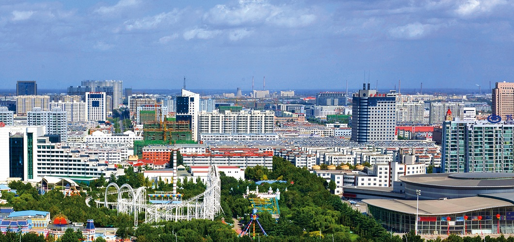
Weifang Photoelectric Industrial Park is an R&D and production base for science and technology enterprises specializing in optoelectronics and electro-acoustics.
The park has a planning area of about 667 square meters with a total investment of 22 billion yuan.
After 10 years of development, the Weifang Photoelectric Industrial Park has established a science and technology innovation system containing a national science and technology business incubator, four national characteristic industrial bases, a national college students' entrepreneurial base, a photoelectric industry strategic alliance, two national laboratories, two post-doctoral workstations, and three academicians workstations.
Weifang Semiconductor Lighting Product Testing Center is also located in Weifang Photoelectric Industrial Park with a technology exchange market.
The industrial park has attracted two candidates of the Recruitment Program of Global Experts, four candidates of Taishan Scholars Program of Shandong Province, three candidates of Weifang high level talent introduction plan for innovation and job creation and nearly a hundred doctors.
Cooperation Mode
Enterprises are allowed to settle in the center through registration.
Contact Person
Sun Hongtian
Phone Number: 13562688823